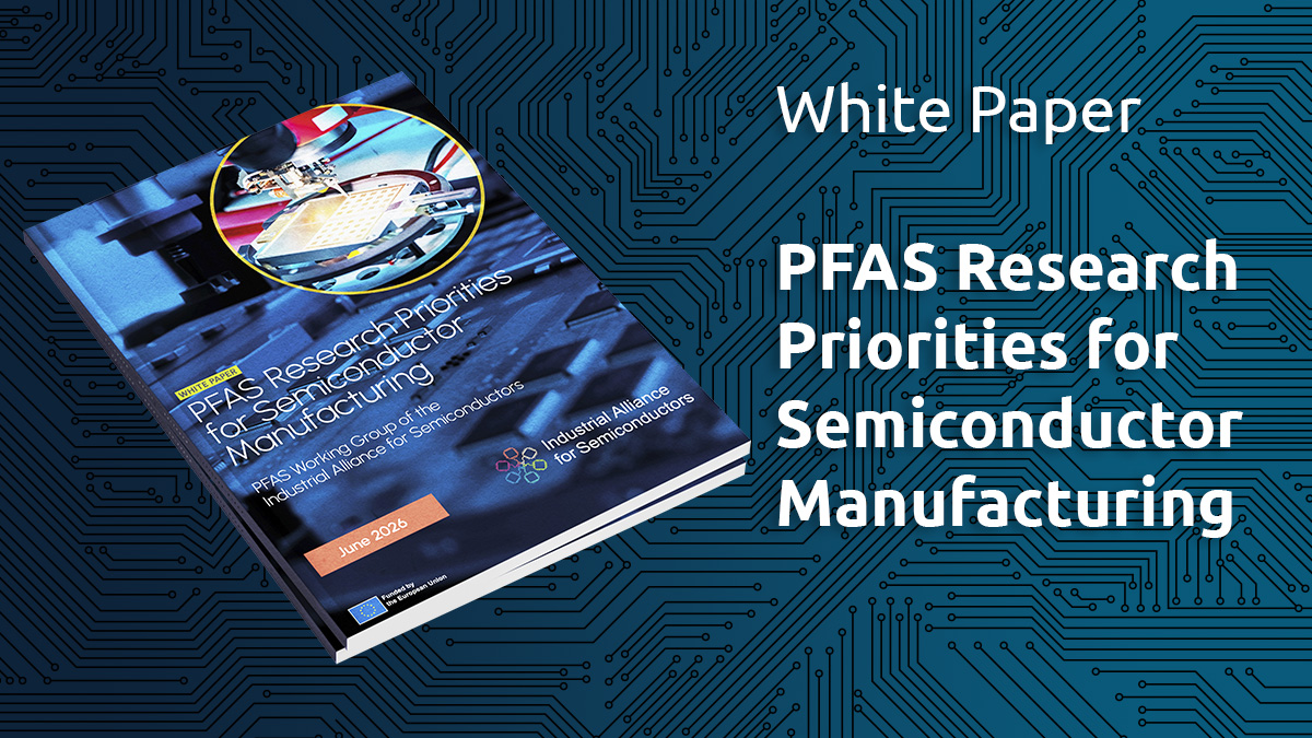
This White Paper is the first deliverable of the PFAS Working Group of the Industrial Alliance for Semiconductors. The document aims to inform future research programmes under the Chips Joint Undertaking (Chips JU) and the 10th Framework Programme (FP10), providing a coordinated roadmap for accelerating technological solutions that support both industrial competitiveness and environmental sustainability.
Download the White Paper
Semiconductor manufacturing relies on a wide range of highly specialised materials, chemicals, and manufacturing processes that require exceptional levels of reliability, precision, and performance. PFAS currently play a critical role across many stages of semiconductor production due to their unique chemical and physical properties, including high thermal and chemical stability, low surface tension, excellent electrical characteristics, and long operational lifetimes. These characteristics make PFAS indispensable for applications such as photolithography, plasma etching, wafer processing, manufacturing equipment, cleanroom infrastructure, and advanced device packaging.
At the same time, the semiconductor industry recognises the environmental concerns associated with PFAS persistence and supports the long-term objective of reducing dependence on these substances wherever technically and economically feasible. However, the White Paper emphasises that this transition cannot be achieved through short-term regulatory measures alone. Many of the technologies required for effective monitoring, emissions control, destruction, and substitution remain at relatively low levels of technological maturity and require sustained investment in research and innovation before they can be deployed at industrial scale.
The document identifies three interconnected research domains that should guide future European investment.
The first concerns PFAS detection and monitoring. Current analytical methods provide high levels of accuracy but remain expensive, laboratory-based, and unsuitable for continuous industrial monitoring. Existing techniques often require lengthy sample preparation and are unable to provide real-time information on PFAS concentrations within semiconductor manufacturing processes. The White Paper therefore highlights the need to develop in-line monitoring systems, advanced sensing technologies, and analytical methods capable of detecting a broader spectrum of PFAS compounds across wastewater, exhaust gases, and solid waste streams. Improved monitoring would support both regulatory compliance and early intervention by enabling continuous process control and more effective emissions management.
The second research priority focuses on PFAS abatement, capture, destruction, and circularity. While several technologies already exist to remove or destroy PFAS emissions, many remain energy-intensive, costly, or insufficiently effective when applied to the highly complex waste streams generated by semiconductor manufacturing. The White Paper identifies important research gaps in airborne emissions control, wastewater treatment, and solid waste management, calling for the development of more energy-efficient destruction technologies, hybrid abatement systems, intelligent monitoring and control solutions, and scalable treatment infrastructures. It also highlights the importance of circular economy approaches, particularly for fluoropolymers, through improved sorting, recycling, depolymerisation, and material recovery strategies that can reduce both environmental impacts and resource consumption.
The third area addresses the development of alternatives to PFAS. Replacing PFAS represents one of the most technically demanding challenges facing the semiconductor industry, as alternative materials must replicate a unique combination of performance characteristics without compromising manufacturing reliability or device quality. According to the White Paper, research efforts should initially concentrate on applications where substitution offers the greatest potential, including photolithography chemicals, plasma etching gases, manufacturing equipment components, cleanroom infrastructure, protective coatings, and advanced packaging materials. The document also stresses the importance of rigorous validation, life-cycle assessment, and collaboration between semiconductor manufacturers, equipment suppliers, material producers, and research organisations to ensure that alternative solutions do not introduce new environmental or technical risks.
Beyond these three technical priorities, the White Paper places significant emphasis on the broader regulatory context. PFAS regulation is evolving rapidly across Europe and internationally, with increasing attention given to emissions reduction, product restrictions, supply-chain transparency, and lifecycle management. While regulatory approaches differ across jurisdictions, the overall policy direction reinforces the need for proactive investment in research that enables industry to anticipate future requirements while maintaining technological leadership and industrial competitiveness.
Building on this analysis, three overarching strategic priorities emerge.
• First, Europe should strengthen investment in research and innovation that accelerates the development of reliable monitoring technologies, scalable abatement systems, and high-performance PFAS alternatives capable of meeting the demanding requirements of semiconductor manufacturing.
• Second, closer coordination between industry, research organisations, policymakers, and public funding programmes will be essential to translate scientific advances into industrial deployment. Long-term collaboration across the semiconductor value chain can help bridge existing technology gaps and accelerate the transition from laboratory research to high-volume manufacturing.
• Third, future European funding instruments should adopt an integrated approach that combines environmental objectives with industrial competitiveness. Supporting research on PFAS should not only reduce emissions and environmental impacts but also reinforce Europe's technological capabilities, supply chain resilience, and strategic autonomy within the global semiconductor ecosystem.
In conclusion, the White Paper argues that reducing the semiconductor industry's dependence on PFAS represents a long-term technological challenge that requires coordinated action rather than isolated interventions. Progress will depend on sustained public and private investment, robust collaboration across the European innovation ecosystem, and the development of practical solutions that balance environmental protection with the performance requirements of advanced semiconductor manufacturing. By defining clear research priorities, the document provides a common framework for guiding future European investment and supporting the transition towards more sustainable semiconductor technologies.
